首页 > NEWS > Industry News
【summary】
Shuttling flow cells smaller than a drop of blood to functional areas is fundamental to the development, automation, and miniaturization of powerful in vitro diagnostic (IVD) systems. These systems in turn support a wide range of applications and devices, from digital biology to next -generation genome sequencing, organs-on-a-chip, high-throughput cell-based assays, and high-density multifunctional chips for drug discovery and bioanalysis.

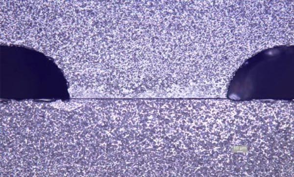
Figure 1. >0.3 mm glass wafer with isotropically etched channels bonded to 1 mm thick glass wafer with room temperature UV adhesive; glass:glass bond preserves bioactivity of encapsulated biomolecules/cells.
Shuttling flow cells smaller than a drop of blood to functional areas is fundamental to the development, automation, and miniaturization of powerful in vitro diagnostic (IVD) systems. These systems in turn support a wide range of applications and devices, from digital biology to next generation genome sequencing, organs-on-a-chip, cell-based high throughput analysis, and high density multifunctional chips for drug discovery and bioanalysis.
The goals of reducing sample volume and reagent consumption, increasing assay speed, and lowering costs are pushing IVD device manufacturing to a new limit while increasing device complexity and functional integration. Their size and complexity present significant challenges, and post-manufacturing modifications such as coatings can also impact the production process and cost.
The materials used in IVD devices define not only the patterning and processing of the application, but also the manufacturing, performance, functionality, and cost of the device. Glass and glass hybrid materials are typically the best performing and most expensive consumables in the device due to advances in processes such as laser processing, lithography, etch automation, wafer bonding, functionalization, room temperature UV adhesive bonding, etc.
Feature Size and Design Complexity
As dimensions decrease, surface anomalies once considered defects can function, and wafer processing techniques can produce features on the same scale as biopolymers and cellular structures. Reactive ion etching (RIE) creates cellular and biomolecular docking sites in glass, and increased surface roughness can be coupled with molecular recognition elements (if appropriate) to improve selectivity. Nanofluidics confine volumes in submicron channels to exploit small-scale phenomena.
While soft lithography polydimethylsiloxane (PDMS) is common in academic research, the mechanical, chemical, and optical properties of glass offer many advantages over these materials. For example, wall stiffness and stability help nano- or micro-channels withstand bonding or sealing, and the ability of bonded glass to withstand flow pressures is key. Many applications benefit from glass鈥檚 thermal properties, chemical stability, and negligible autofluorescence. Finally, the glass surface can be infinitely tuned through silanization reactions to achieve a wide variety of properties.
While silicon is often the best material for confining individual cells or creating high aspect ratio features required for specific flow sections, glass can often be used as a substrate when other properties of glass (such as optical smoothness, dielectric constant, metal layer processing step requirements, bonding methods, etc.) are required. Processing techniques from the semiconductor industry can create high-aspect ratio micro- and nanochannels, with aspect ratios as high as 20:1 demonstrated in glass using a combination of laser micromachining and chemical etching. Extensive work describing surface modifications in glass has shown that glass, as a substrate, has the most chemically tunable surface to date.
Biological applications sometimes require the integration of optical devices, optical windows, electrodes, electronics, and 3D structures such as barriers or pores. Combining subtractive techniques such as ultrafast laser fabrication and chemical etching with additive methods such as electroless plating and CVD allows the fabrication of complex, multifunctional chips in glass and fused silica, including those on polymer surfaces, with each material facilitating specific applications and design parameters. Because hybrid material devices can overcome the challenges of working with living cells, the best solution is often to exploit the properties of each material.
The choice of materials, configurations, and post-fabrication processing for chip-based IVD cell culture systems depends on the cells, culture media, and phenomena to be observed. Even the channel design can affect cell viability, as some cells are more susceptible to shear stress than others. PDMS is often used because its permeability allows for gas exchange between cells on the chip and with the chip鈥檚 surrounding environment. However, this property can compromise cell health when gases and ions migrate unexpectedly. Similarly, patterning cells to position them in one area of the device has many advantages, but the cells may ultimately suffer because the surface can affect cell shape and physiology.
Neuronal cells are often measured with electrodes, making standardized patterning of electrodes on glass or silicon a reason to choose any material. The capabilities of transparent gallium tin oxide (ITO) electrodes tip the balance toward glass, as they allow cells to be monitored with a microscope, even at the electrode surface.
Glass is generally the best material for optical methods and can be used with UV adhesives at room temperature, which are well known in the industry and have validated biotoxicity and biocompatibility data (see Figure 1).
Cell Adhesion and Sorting
Methods to confine cells to specific areas include micro- and nano-patterning of surfaces and the use of TMMFs, a type of photostructured material, to create so-called 2.5D structured interlayers to capture and culture cells. Another strategy is to use self-assembled monolayers (SAMs) to define surface functionality for adhesion, lubrication, wetting, or physical adsorption of proteins. Thiol-based SAMS react with gold, a metal that is easily patterned on glass. Silanes are another well-known glass reactive chemistry tool that enables important surface modifications for IVDs, including increasing hydrophobicity for cell/biomolecule adhesion or droplet/digital microfluidics; increasing hydrophilicity to prevent biomaterial adsorption; and adding surface charge for ion association or other purposes.
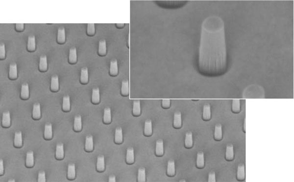
Recent studies have shown that manipulation of cell geometry, such as circular or square patterning, can affect key cellular processes. Deep reactive ion etching (DRIE) can pattern silicon, quartz, or glass wafers for silicon micropillar arrays (see Figure 2).

Figure 2. Nanopillars in glass increase the surface area for interactions.
Similarly, photoimageable adhesives (PBAs) allow for the direct realization of economical and complex fluidic channel systems on glass using standard MEMS processes.
Widely used for sorting heterogeneous cell populations. Within the three categories of cell sorting (fluorescent label-based, bead-based, and label-free) there are a variety of selection mechanisms: photomechanical, electrical, acoustophoretic, magnetic, mechanical, or passive.
Depending on the fluorescence efficiency of the target, wavelength, and limit of detection (LOD), glass or fused silica generally perform best due to their low autofluorescence, even if other materials (such as electrodes) are required. Label-free methods are not necessarily exempt from the optical clarity and low autofluorescence requirements that drive glass selection. If intrinsic fluorescence, optical, or optoelectronic tweezers are used, glass or glass hybrids are usually best.
Applied Genomics
As with other biological measurements, the best material for high-throughput and low-volume nucleic acid analysis depends largely on the detection mechanism and the thermal properties of the material. Glass, for example, is ideal, and as a substrate, it has other attractions: optical glass or fused silica do not strongly inhibit polymerase chain reaction (PCR) enzymes, nor do they off-gas or absorb water or ions that could contaminate the enzyme reaction.
A major innovation in achieving the $1,000 genome goal has been the recognition of the role of sample preparation, including the expansion and quantification of DNA libraries using digital PCR (dPCR), a method that partitions samples into single-molecule partitions. Such small partitions make quantification on the order of small percentages possible.
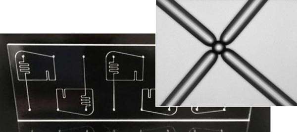
The critical ability to generate thousands to millions of droplets depends primarily on the design and fabrication of digital microfluidic chips (see Figure 3). The resulting accuracy and selectivity are aiding understanding of complex expression patterns in cancer and other diseases, as well as therapeutic and diagnostic approaches such as liquid biopsies.

Figure 3. The production of pressure-driven droplet microfluidic components depends on the excellent surface properties of glass: low surface roughness, chemical inertness, and high-precision manufacturing tolerances to ensure reproducible droplet volumes.
Glass plays an important role in fabricating pressure-driven droplet microfluidic components because of its low surface roughness, high chemical inertia, and precision manufacturing tolerances. In addition, due to its renowned surface chemistry, it is relatively easy to create hydrophobic areas on hydrophilic glass to produce uniform droplet volumes and aid droplet separation.
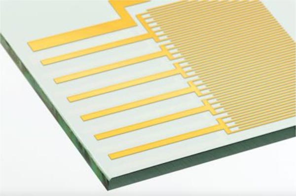
Digital microfluidics utilizes electrode arrays and electrowetting to generate droplets and control their size and motion. Therefore, glass is the best material because the required high-density ITO electrodes can be easily patterned on glass (see Figure 4).

Figure 4. High-density indium tin oxide (ITO) electrodes are easily patterned on glass.
Many next-generation sequencing (NGS) technologies use optical methods that exploit the optical properties of glass. A key technology in achieving the $1,000 genome is to build up a glass surface to create a patterned flow cell. Patterning can significantly reduce image acquisition time. An important factor in this success is the accuracy of submicron wafer-scale patterning, which enables extremely dense packing of sequencing spaces in microfluidic chips, reaching the optical resolution limit of traditional fluorescence imaging systems.
While label-free analysis would appear to eliminate the need for the optical properties of glass, glass still has some advantages. For both silicon and glass, submicron control of channel etching depth can improve the signal-to-noise ratio of impedance detection. ITO electrodes can be easily integrated to integrate digital microfluidic sample preparation, helping to reduce precious sample and expensive reagent consumption.
Whatever the application, IVD developers must balance the requirements of biology and device engineering. In any case, the basic step of selecting the circulating cell material can have a large impact.
| Free solutions/free proofing 13710252340
Previous: Understanding laser welding te