首页 > NEWS > Industry News
【summary】
The surface of sapphire substrate is hard, and the general cutter wheel is difficult to cut, wears out, and has low yield rate. The cutting path exceeds 30m, which not only reduces the use area, but also reduces the production of products. In the LED industry driven by LED, the demand for sapphire substrate wafer cutting has increased, and higher requirements have been put forward for improving production capacity and finished product qualification rate.
The surface of sapphire substrate is hard, and it is difficult to cut with general cutter wheels, which causes wear and tear, and has a low yield rate. The cutting path exceeds 30m, which not only reduces the use area, but also reduces the production of products. In the LED industry driven by LEDs, the demand for sapphire substrate wafer cutting has increased, and higher requirements have been put forward for improving production capacity and finished product qualification rate.
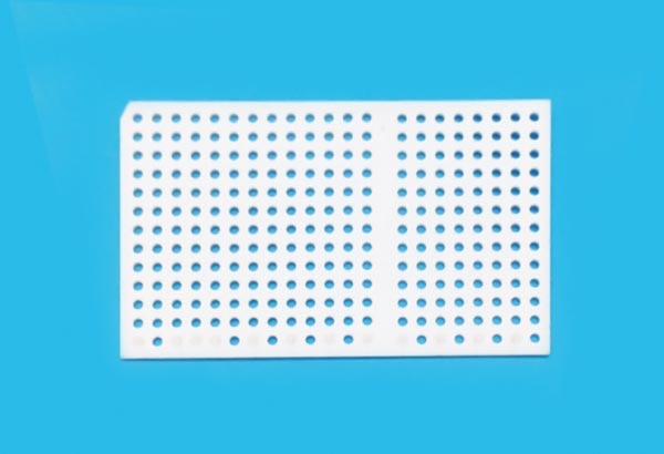
UV laser ceramic cutting
In the last century, the application of electronic ceramics gradually matured and had a wider range of applications, such as heat sinks, piezoelectric materials, resistors, semiconductor applications, biological applications, etc. In addition to traditional ceramic processing technology, ceramic processing has also entered the field of laser processing due to the increase in application types. According to the material type of ceramics, they can be divided into functional ceramics, structural ceramics and bioceramics. Carbon dioxide laser, YAG laser, green light laser, etc. can be used for ceramic processing. However, with the gradual miniaturization of parts, UV laser processing has become a necessary processing method for processing various ceramics.

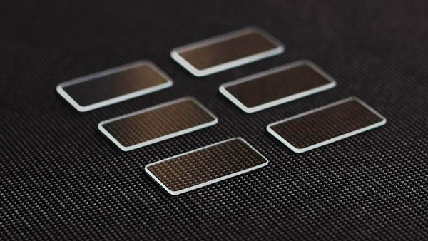
Glass UV Laser Cutting
Driven by the rise of smart phones, the application of ultraviolet lasers has gradually gained room for development. In the past, because mobile phones had few functions and high laser processing costs, laser processing did not have much status in the mobile phone market. But now smart phones have high functions and high integration, integrating dozens of sensors and hundreds of devices in a limited space, and the cost of components is very high. Therefore, the requirements for accuracy, yield and processing have been greatly improved, and ultraviolet lasers have developed a variety of applications in the mobile phone industry.

UV laser ITO dry etching
The most notable feature of smart phones is the touch screen function. Capacitive touch screens can achieve multi-touch, corresponding to resistive touch screens, long service life and fast response speed. Therefore, capacitive touch screens have become the mainstream choice for smartphones.
In the past, ITO lines were wet etched. The lines were treated with yellow light, and then the ITO film on the surface was removed with etching liquid to form the lines, which was time-consuming and polluting.
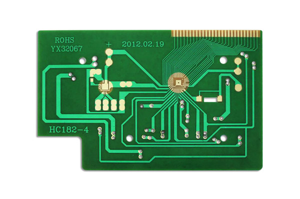
UV laser cutting circuit boards
Laser cutting circuit boards was first used for flexible circuit board cutting. Due to the wide variety of circuit boards, early processing used mold forming, but the mold production cost was high and the production cycle was long. Therefore, UV laser processing can eliminate the mold production cost and cycle, greatly improving the proofing time.

| Free solutions/free proofing 13710252340
Previous: Market analysis of precision l