首页 > NEWS > Industry News
【summary】
All of these technologies have one thing in common 鈥?they all rely on a printed circuit board (PCB) to deliver functionality. PCB depaneling is the process of removing many smaller individual circuit boards from a larger panel during manufacturing. Laser depaneling is a non- contact process, which means that standard SMT carriers can be used throughout the production process.
We are surrounded by technology every day, and we want to be your preferred laser equipment supplier in the production of the latest technology.
Think back to all the devices we use in a day: our phones, our TVs, the computers we use; the systems in our cars that deploy airbags or life-saving medical treatments. All of these technologies have one thing in common - they are all delivered by printed circuit boards (PCBs).
What is Laser PCB Depaneling?
PCB depaneling is the process of removing many smaller individual circuit boards from a larger panel during manufacturing.
The laser process used frees delicate components, solder connections and fragile substrates from any mechanical stress. With minimal space between boards, each panel is worth more. Additionally, components can be placed next to each other to minimize unnecessary volume and weight.
PCBs are often manufactured in large panels with multiple boards, but can also be produced as single units. The depaneling process can be fully automatic, semi-automatic or manual. This results in lower production volumes while eliminating the additional costs of tooling and waste removal associated with mechanical methods.

Why is PCB important?
Without PCB, electronic design would be impossible. These technologies support and connect all electronic components, allowing data to run and get better calculations.
As integrated circuit (IC) manufacturing continues to advance, the number and density of connections connecting devices continues to increase.
To further help increase the yield of PCBs while still maintaining a small size, various depaneling techniques were created.
What are the typical PCB depaneling methods?
1. Knife die traditional punching/die cutting
This process requires a different chip for each new circuit board. One part of the punching fixture has a sharp blade and the other part has a support.
It also uses a shearing or crushing method, which can deform the board. Sharp die edges are essential to minimize damage.
2.V-Shaped Split
Screaming the board along the cut lines on both sides can reduce the thickness of the board. The depth of the score on both sides of the panel is about 30% of the board thickness. The PCB is then removed from the panel.
3. Wheel Cutter
This is a manual alternative method that cuts the fabric after the V-shaped score to cut the remaining fabric. This method requires careful alignment between the V-shaped score and the knife wheel to reduce stress on certain components.
4. Sawing
A single routing saw blade is usually used to cut panels from the top or bottom.
5. High-pressure water cutting
This technology has not been fully explored, but the cutting is done by a high-speed mud stream.
The slurry is a mixture of water and abrasive, and the method is followed by washing to remove the abrasive part.
6. Curve (Routing board splitter)
Most PCBs are routed so that the individual circuits are connected to the panel frame through narrow tabs. The tabs are broken or broken to separate the circuits.
7. Laser Cutting
This method does not require mechanical molds or blades and is completely controlled by software.
Paths of any shape, including curves and sharp corners, can be completed using this method, which also provides unparalleled space advantages.

In each of the above methods, except laser cutting, a certain degree of mechanical stress is applied to the board. This applied stress can cause delamination or lead to space development. These methods also require the removal of the final connection between the board and the panel. Bending stresses can damage components close to the necessary removal area.
Laser cutting offers all of the following benefits:
1. Temperature:
An experienced engineer can achieve the perfect settings to ensure a clean cut with no burn marks. Material type, thickness, and condition are all factors to consider and will determine the speed (and therefore temperature) of the laser.
2. Exhaust:
An exhaust or filtration system can remove any expelled material during the laser process.
If the application does produce very small particle residue, compressed air or a smooth paper towel can be used.
3. Pressure:
Since there is no contact with the panel during the cutting process, the laser allows all most or all depaneling to be done after assembly and soldering. This avoids any bending or pulling of the board so no stress is applied and no damage occurs.
Reduce production costs with fast and easy setup
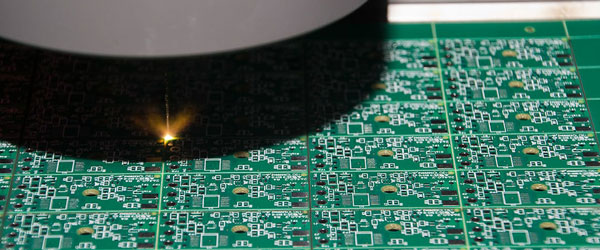
Laser depaneling is a non-contact process, which means that standard SMT carriers can be used throughout the entire production process. No special jigs or fixtures are required, as the only mechanical force acting on the board is caused by the handling equipment. Laser depaneling is also able to process boards with components assembled on both sides.
Our lasers cut the substrate next to the delicate components without causing any mechanical stress. This allows small applications with populations up to the edge of the printed circuit board to be expertly processed. Due to the tight tolerances, the occurrence of scrapped products is also minimized.
Due to the trend towards smaller and smaller components in current technology, laser depaneling can meet the needs of any project. The focus of the laser beam is ideally suited for very narrow channel cutting, saving space and material.
When to Use a Laser Depaneling
Laser depaneling is ideal for micro-machining metals, plastics, ceramic materials and material combinations. Some specific applications include drilling holes in HDI circuit boards, TCO/ITO structuring, laser removal of tin resist, drilling holes in flexible materials, openings in solder resist, and laser repair and rework of printed circuit boards.
The need for complex tools or adapters is eliminated, only the layout data needs to be uploaded. Small, sensitive PCBs with limited space on the panel are ideal applications, improving handling capabilities and quality.
How is PCB depaneling done?
Laser depaneling is fast, precise, with no tooling costs or wear, no parts-induced stress, and no cutting oil or other waste. The non-contact depaneling method using lasers provides highly accurate segmentation without any risk of damaging the material, regardless of the substrate.
As the technology world continues to innovate and create smaller, more advanced devices, Laisse offers the latest in precision parts manufacturing to meet this demand.
| Free solutions/free proofing 13710252340
Previous: Abrasive tool cutting machine