首页 > NEWS > Industry News
【summary】
Industrial picosecond lasers are ideal for scribing, cutting, and drilling thin films. High average laser power, very high repetition rates, and 24/7 reliability combine to deliver superior quality, higher yields, and lower costs for thin films made from metals, semiconductors , plastics, and dielectrics.
Industrial picosecond lasers are ideally suited for scribing, cutting, and drilling thin films. The combination of high average laser power, very high repetition rates, and 24/7 reliability results in superior quality, higher throughput, and lower costs for thin films made from metals, semiconductors, plastics, and dielectrics. In this article, we will examine some example applications in photovoltaics鈥攁n industry that requires the 24/7 processing and high throughput of traditional microelectronics, but at one-tenth the cost.
Emerging Applications in Thin Film Solar Devices
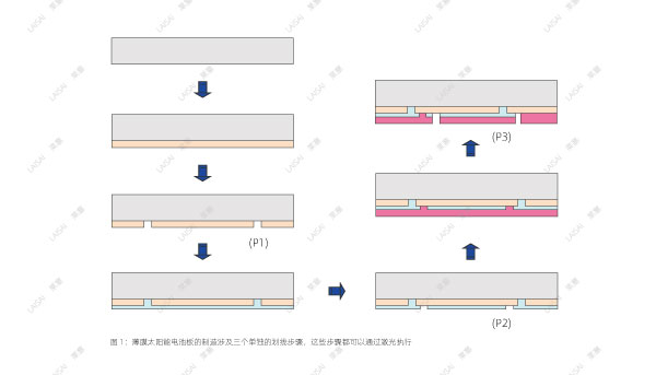
While crystalline silicon devices currently have the largest market share, thin film solar is an important alternative that is growing steadily as it involves lower material costs and offers the promise of deployment on curved and/or flexible surfaces. There are several different types of thin film solar products, with various manufacturers preferring different semiconductor materials as well as different panel sizes. All thin films currently produced rely on a series of scribing steps, referred to as P1, P2 and P3, which are used to pattern the various layers after vapor deposition 鈥?see Figure 1 (all rigid products are based on having a thickness in the 2-3 mm range).

By alternating vapor deposition and scribing, the semiconductor and conductor layers are patterned to create active strips of 5-10 mm x >1000 mm that are physically connected in parallel but electrically in series. In this way, the entire panel is capable of producing hundreds of watts of power.
The first step is to deposit a uniform (a few hundred nanometers) layer of transparent conductive oxide (TCO) on the glass, which will form the front electrode, through which sunlight passes to reach the active semiconductor layer. The TCO is then patterned by a P1 series scriber, which must cut through the entire TCO thickness. The p-type and n-type semiconductors are then deposited, with a total thickness of 2-3 microns. The P2 scriber then cuts the semiconductor layer, dividing it into active strips. A thin (< 1 micron) layer of metal (aluminum or molybdenum) is then deposited over the entire panel to form the back electrode. This is patterned by a P3 scriber, which cuts through both the metal and semiconductor layers.
Why Picosecond Laser Processing?
Photovoltaic panel manufacturing requires closely spaced narrow scribe lines to minimize wasted (inactive) panel area, as shown in Figure 1. But this also means that the application cannot tolerate peripheral thermal or mechanical damage, such as micro-cracks or chips.
Nanosecond lasers have proven well suited for P1 scribers that remove hundreds of nanometers of TCO. However, P2 and P3 scribing involves thicker layers (semiconductor or metal), and the challenge is to completely cut through these layers without causing thermal damage to nearby or underlying materials. Picosecond lasers are well suited for this task because the pulse width is short compared to the thermal diffusion time; thermal damage is minimized through cold picosecond ablation, eliminating the possibility of shorts. Equally important, commercially available mode-locked lasers offer extremely high repetition rates and high average powers (up to 100 W). The combination of low pulse energy and high repetition rate also provides high throughput while eliminating the chance of functional damage to the panel. Picosecond lasers are now also available in a variety of wavelengths, which allows the use of a highly efficient thin-film patterning technique called spalling for P2 and P3. In this process, the laser wavelength is chosen so that it passes through the glass and TCO but is strongly absorbed at the interface with the semiconductor (for P2) or metal (for P3). This evaporates several atomic layers of the material, completely removing the overlying layer in a single laser pulse (Figure 2).

Picosecond Processing Proven in c-Si Solar
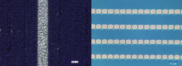
Picosecond laser scribing and dicing has previously been successfully used in the production of c-Si solar cells, for example to create openings through the SiN passivation layer to allow direct electrical connection to the active semiconductor layer. In some cases, the application requires a long, continuous groove. This can be created by using a beam with a Gaussian profile and then overlapping the pulses - see Figure 3 (left). However, some SiN on Si scribing applications require avoiding any pulse overlap to completely avoid any damage to the underlying silicon. Figure 3 (right) shows an example using a beam with a uniform profile that is shaped using top-hat optics. The closely spaced square holes in the (<100 nm thickness) SiN shown here confirm that the ps laser also does not cause lateral thermal damage to the SiN. In these single-pulse applications, the high repetition rate of the ps laser (up to 5 MHz) means that the limiting factor is the scanning speed. Galvo scanners can deliver speeds of up to 30 m/s, equivalent to 1 million holes/second. Faster polygon scanners can increase the speed to several million holes/second.

Cutting Glass Modules
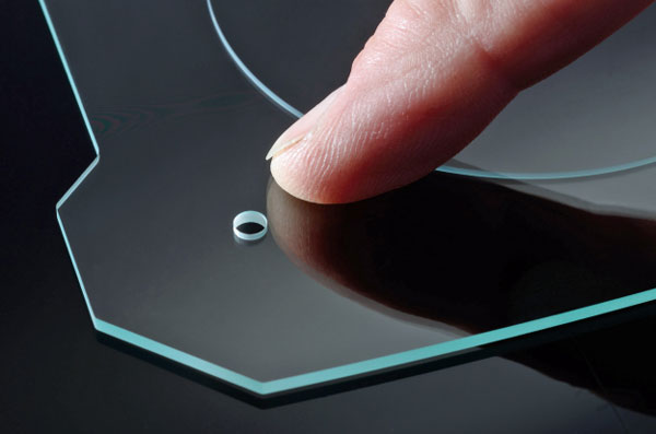
The encapsulation of solar devices also benefits from picosecond lasers. Specifically, a unique glass-cutting filamentation method called Smart Cutting enables rapid cutting of tempered glass in a cold process, resulting in tight curves and holes - see Figure 4 - and typically with excellent edge quality (Ra < 0.5 渭m) without post-processing. In short, as the picosecond laser beam passes through the thickness of the glass, it automatically oscillates between focused and unfocused, drilling a narrow micro-perforation in the glass. The movement of the glass and/or the laser forms a curtain of these filaments that define a smooth break that, in some glass types, does not even require any type of impact to separate. Unlike mechanical cutting, the edges are free of microcracks and residual stresses, eliminating common failure mechanisms for thin glass panels.
In Summary
Like most other electronics-related industries, the photovoltaic market has a growing demand for precision micromachining to improve performance, yield, and cost. Picosecond laser cuttingis proving to be the ideal tool for multiple tasks in this important industry.
| Free solutions/free proofing 13710252340
Previous: Laser perforation process that